For applications such as tethered drones that require a wide voltage range and high-efficiency, high-density converters, the ZJU-PMIC team previously proposed an input-series output-parallel (ISOP)cellular DCX scheme, as shown in Figure 1. It reduces device losses caused by high electrical stress and adopts a half-bridge topology with X7R surface-mount capacitors as resonant capacitors to improve power density.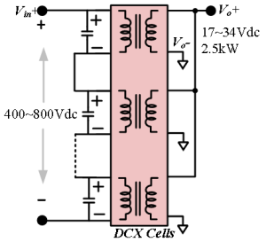
Fig.1 Cellular DCX topology
In short, when the output voltage is low,insufficient magnetizing current and mismatch between the resonant and switching periods are the main causes of increased losses.
Among these, the magnitude of the magnetizing current is positively correlated with the duration of the switching period. When the output voltage is low, a longer switching period is needed to energize the magnetizing inductor and achieve ZVS of the switches; at the same time, a low output voltage increases the resonant capacitance, which increases the resonant period. This means that when the output voltage is low, increasing the switching period duration is expected to simultaneously solve the problems of ZVS loss and mismatch between the resonant frequency and switching frequency. To this end, ZJU-PMIC established a model in which the frequency for achieving ZVS (fzvs) and the resonant frequency (fr) vary with output voltage, as shown in Figure 2.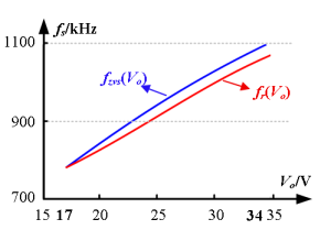
Fig.2 fzvs and fr vary with output voltage in basically the same way
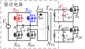
Fig.3 Variable-frequency resonant driving
Figure 4 presents the key waveforms of the driving circuit and the main circuit, including the waveforms of the driving circuit and the main circuit.
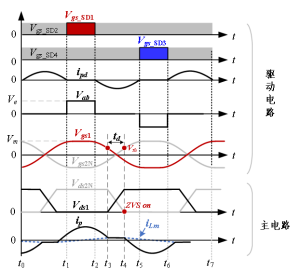
Fig.4 Key waveforms of the variable-frequency resonant driving and the main circuit
The entire operating cycle is divided into two clamping stages and two resonant stages. Changing the duration of the clamping stages changes the duration of the entire switching cycle, thereby achieving the variable-frequency function. The two clamping stages and the resonant stages are shown in the figure below.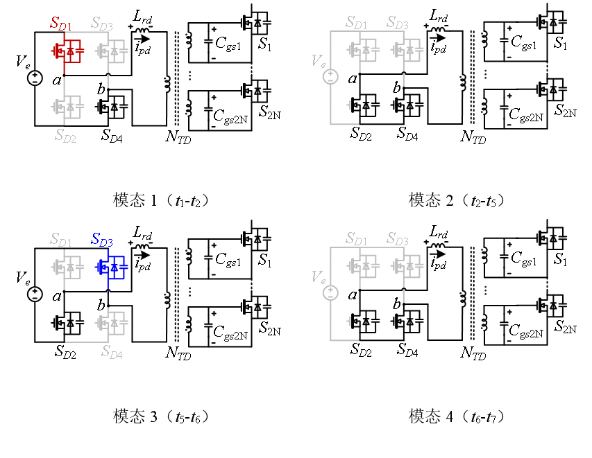 Fig.5 Equivalent circuit diagrams of the variable-frequency resonant driving under different modes
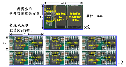
Fig.6 Voltage-mode driving scheme and current-mode driving scheme
Verification of the key waveforms of the resonant circuit and the consistency of multiple output signals is shown in Figure 7 and Figure 8.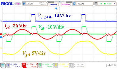 Fig.7 Key waveforms of the resonant driving circuit
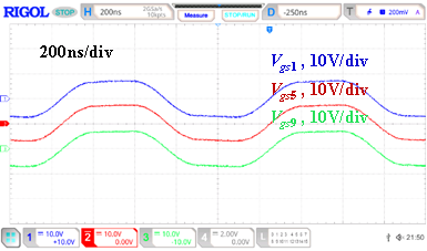
Fig.8 Consistency of multiple driving signals
Based on this resonant driving technology, the wide-voltage-range high-efficiency high-density cellular DCX prototype has an input voltage of 400-800Vdc, an output voltage of 17Vdc-34Vdc, a power density of 1.6kW/in³, a peak efficiency of 99.0%, and an efficiency of 98.3% at 2.5 kW full load.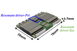
References: X. Wu, S. Gao and X. Huang, “99% Peak Efficiency MHz Cellular DCX Considering the Nonlinear Parasitic Capacitance for Different Output Voltages,” in IEEE Transactions on Power Electronics, vol. 41, no. 6, pp. 8830-8838, June 2026